After the upper case and key switches were put together I started wiring. I started by following the guide on dactyl git repository but the lack of updates and details quickly drove the project in to the ground. My original intention was to minimize learning and just to blindly follow the guides.
That attitude got me to waste an expensive teensy controller. Then I ordered a pro-micro thinking since it used the same controller it would just be a drop in replacement at half the price. That turned out to be a fortuitous mistake as it made me switch to QMK and made me learn quite a bit along the way.
Back to wiring… I chose a column driven matrix. Chose is a bit ludicrous as at that point I was blindly following the guide. I used the diode legs to form the column wiring. The solid wires made for a neat and orderly column structure.

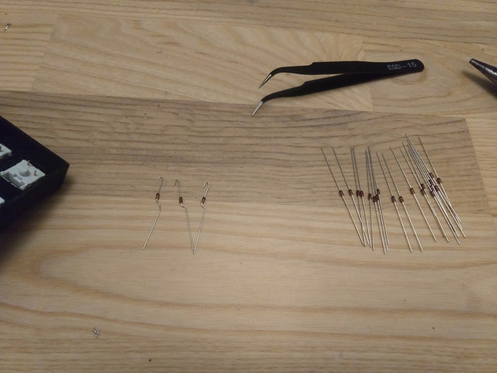
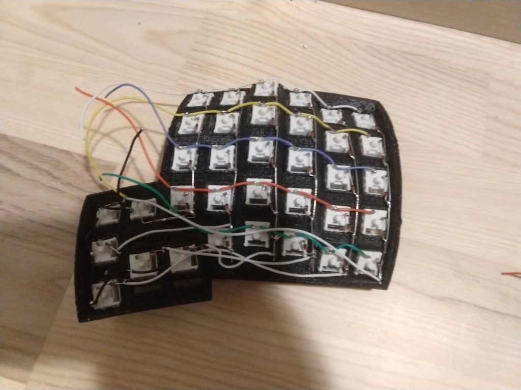
Next up was the rows. I had some wires laying about from a Halloween project. Used different colors to color code the rows. Planning for extra cabling on the inside allowed me to place the control board in the space on the lower base. The space in there is precious, as it is very hard to fit anything in there.
I made my first mistake by misplacing resistances. The teensy would appear as a usb device and I was able to flash firmware onto it, but it never worked. Later I noticed even the blink program wouldn’t run. I must have fried the board hard. After that I ordered the promicros.
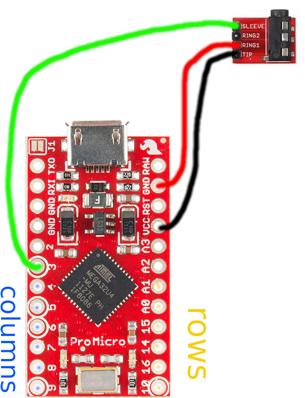
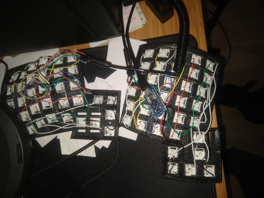
Unlike the teensy build promicro requires two pro micros, one on each half of the keyboard. Each wired and flashed the same way. The two sides are connected via a TTRS cable. The software differentiates the side connected to USB as the right side.
From that point onwards I followed the instructions on QMK git repository. It was very terse and sometimes I had to refer to the source code and compare against promicro instructions but it worked way better than blindly following a guide.
QMK and promicro uses different terminology to refer to pin-outs on the board. On the above picture I marked the columns and rows. You insert column/row 0 on the top port go down increasing the column/row number. So the pin out labeled 4 gets column 0, pin out 5 gets 1, and so on. Pin out A1 gets row 0, A0 gets row 1, and 15 gets 2…
I later added a switch between rst and gnd to ease reseting the board to upload firmware. And that was it for wiring. I had to fix a loose solder, and a reversed diode but that is essentially it.

Leave a comment